YAESU/SOMMERKAMP FT-77S MODIFICATIONS
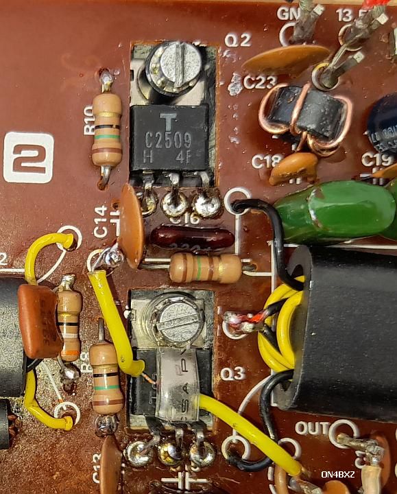
![]() 17-apr-2021 With corrected pins assembly of 2SC2509.
17-apr-2021 With corrected pins assembly of 2SC2509.
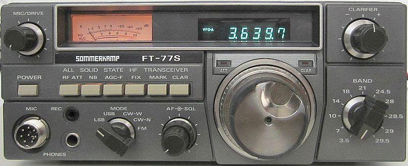
YAESU/SOMMERKAMP FT-77S.
INTRODUCTION
A YAESU FT-77 has an output of 100 W and a FT-77S 10 W. Apart from the power amplifier both devices are identical, even with a SOMMERKAMP frontplate. Just the 160 m band is lacking in both brands.
Although the sets (1981-1987) were advertised as economic transceivers the electrical construction and design were better than the then pasted label suggests.
REPLACE FINAL TRANSISTORS
Two 2SC2509 transistors were "dead" upon a request to "investigate" a FT-77S. Someone had already replaced them, but the collector fin mounted onto the heatsink without insulation. Some things had apparently not gone well.
 |
 |
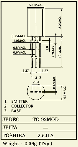 |
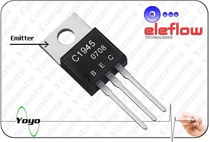
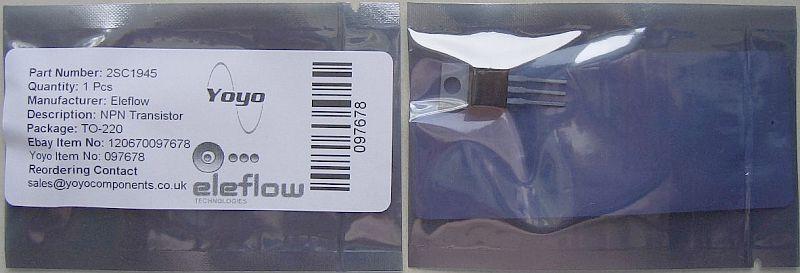
After about 30 years many transistors are obsolete, so it is not always possible to achieve the same or a replacement. One type 2SC1945 seemed interesting because, unlike conventional collector-fin construction, the emitter is connected to the fin and direct installation on mass is an attractive option. According to the data the 2SC1945 has the ability of withstanding infinite load VSWR when operated at 16 V. This transistor has been used in several Asian products as driver stage. There are many fake printed with a Mitsubishi label, which unfortunately does not meet the original specifications. However, one manufacturer (Eleflow) and supplier (Yoyo) (fig») claim to produce and deliver a type with the original specifications: http://www.eleflow.com/2SC1945.pdf
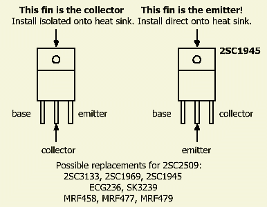
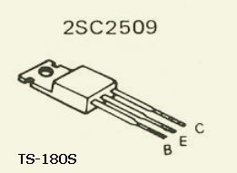
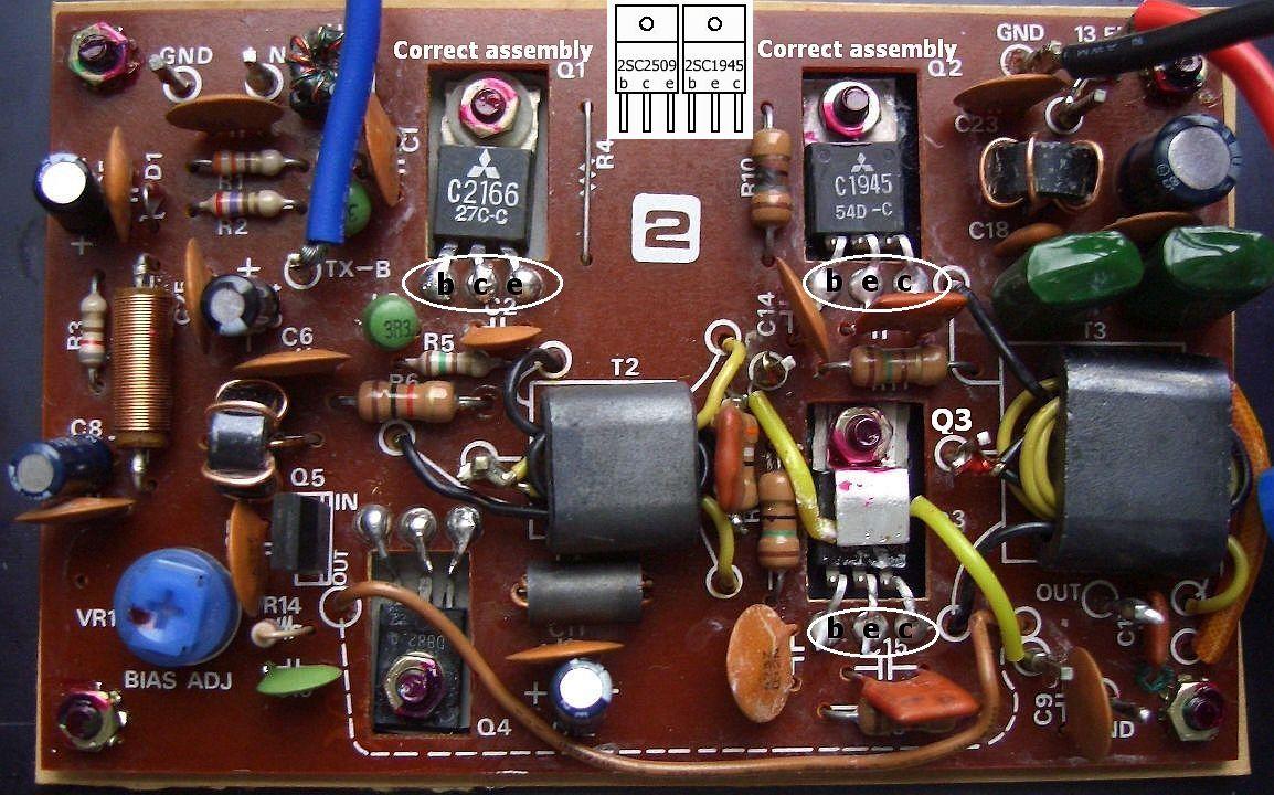
The correct pin connection of a 2SC2509 has been a mystery for years. In various service manuals of for example Kenwood (including TS-180S) it is indicated with images as B, E, C. The emitter is therefore the center pin that is connected to the cooling fin. If one examines the track side of a PCB, it appears that the cooling fin is mounted without insulation onto the chassis or onto a heat sink.
There are two possibilities to explain the problem.
Apparently there are fake 2SC2509's in circulation of which the center pin is the collector e.g.: B, C, E.
It is also possible that the draughtsman of Toshiba's 2SC2509 made a drawing error in the datasheet that no one has noticed, because most TO220 package have the sequence: B, C, E or E, C, B.
If for some reason you need to replace the original output transistors, pay attention to which type you are going to install. If it is a B, C, E then the collector and emitter must be cross-soldered with a mica insulation between collector and heatsink.
If it is a B, E, C type, it can be soldered directly and screwed onto the heat sink without insulation.
It now appears that with 2SC2509 it must be: B, E, C!
INSTALLATION
 |
 |
The board is apparently designed for transistors where the center pin is the emitter and at the same time cooling fin. When mounting the 2SC2509's, the pins of emitter and collector must be arranged crosswise. That will be the reason for failed repairs when installing 2SC2509 transistors.
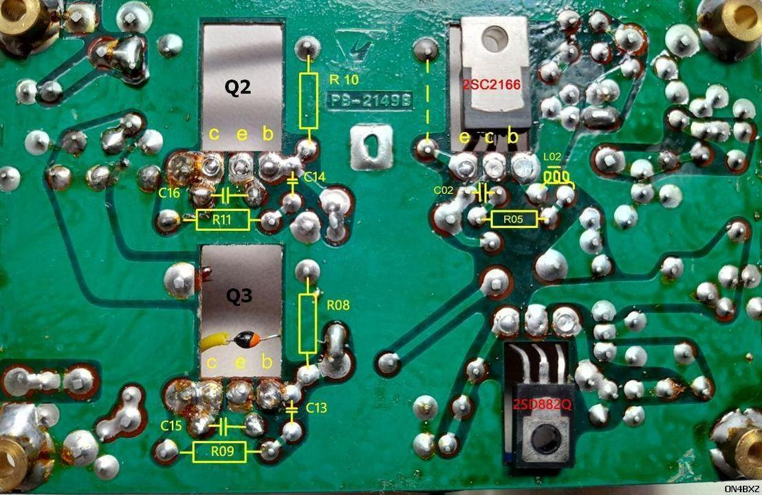
ON4BXZ has found the original 2SC2509 and mounted it on the PCB. The output was 10 W. This shows that with this "vintage" transitor the pin order is: B, E, C!
OUTPUT REDUCED TO 25 W
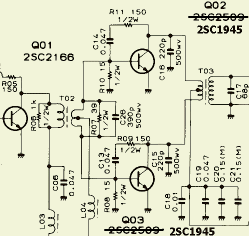
With the new Mitsubishi transistors the output of the FT-77S increased to about 30 W at 13.8 volts and even 35 W on the 15 m band. Given the result nothing of the original design was changed and the power adjusted to 25 W to keep the semiconductors well within the specifications. The («fig) mounting plate of the finals is to small for sufficient cooling so a larger heatsink should be installed.
RF AMPLIFIER
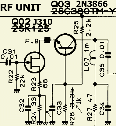
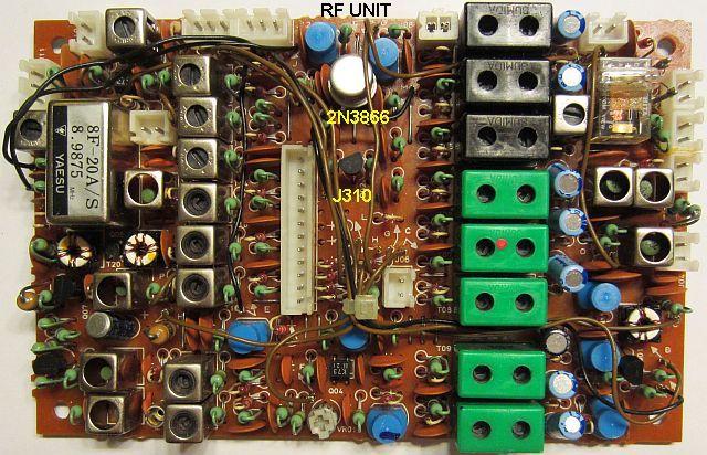
With strong signals on the 40m band the set suffer from seepage of broadcast transmitters outside the amateur band. Probably due to the many switching diodes in the front-end, but also by a "weak" RF amplifier. The latter consists of a cascade amplifier circuit with a FET (2SK125) and a NPN transistor (2SC380) in series.
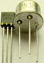
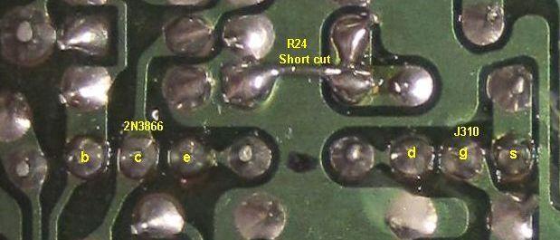
As an experiment I replaced them with more current types: J310 (FET) and 2N3866 (NPN) and shorted R24 (33 Ohm). The connections of both semiconductors are different from the removed components and that is showed («fig) in the pictures.
Unfortunately the overload still exist, but when turning on the attenuated outband broadcast signals vanished. Because I still thought the receiver was improved, the modification was maintained. Anyway after extensive testing by various ways to attenuate the incoming signal, one major improvement was obtained by changing the voltage across the two semiconductors. Instead of 3k3 (R3) 1k was installed. Maybe this was even good for the original components, but I have not bothered to test.
![]()
