I am still experimenting with this design, but the information is sufficient for a home brewer!
![]() 26- jul-2016
26- jul-2016
GU-43B, GU43B, Q-1P/41, Q-1P/42
1.5 KW HF Amplifier FRINEAR 1500
1.8–30 MHz, Input 50 ohm SWR ≤ 1.2
(Passive grid system, PA0FRI's 1.5kW QSK HF LINEAR published in RSGB's RadCom nov 2003)
|
The first design.
The second design. Recent experiments with a stripped design.
Fitted with an electronic bias switch.
|
|
Trial version second design. |
Click to enlarge. |
INTRODUCTION
While the circuit diagram provided the necessary basic information, care must be taken to use suitable rated components, adequate fan cooling etc. Remember always that this is a high power amplifier with potentially lethal (HV) voltages.
|
This experimental design is capable of 1.5 kW output throughout the range 1.8–30 MHz. Delivering 300–400 W output with 5 W of driving power. The input is "swamped" by a non-inductive 50 Ω control-grid resistor eliminating the need for tuned circuits. This match the input circuit on the amateur bands, after band changing, only two capacitors need to be tuned. This type of linear has many desirable features, including low cost, low component count, stability due to the swamping effect of the passive grid input load and simplicity of the construction. |
Testing the trial version, left side: a g2 supply. |

The simple screen supply (fig») incorporates protection circuitry comprised of a small 230 VAC/15 W domestic lamp bulb as a constant current device. If the HV fails or the amplifier is not correctly tuned or is overloaded, the screen grid dissipation is limited to a safe value. If the pi-network output circuit is determined empirically for lowest screen current and maximum output, the screen supply is quite adequate and stable.
In practice, the GU-43B power valve and equivalent Polish-manufactured Q-1P/41 and Q-1P/42 are very rugged. During development of the amplifier; they withstood temporary overload: screen grid current 300 mA, anode current 2 A and 100 W drive without the 6 dB attenuation. The GU-43B is extremely stable in this design; no sign of oscillation even without in- and output loading. Lowest screen-grid current occurs with anode voltage between 3 and 3.3 kV. With normal speech the current should flicker about zero mA (±5 mA). With a carrier (key down), it is about 20 mA positive.
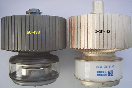
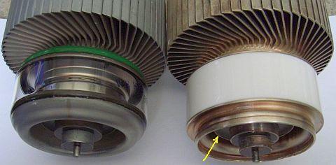
Q-1P/41 is a silver plated GU-43B; Q-1P/42 is a silver-plated and ceramic GU-43B. Both types have a better amplification factor than the Russian GU-43B. They need 1.0 to 1.5 V more negative bias (e.g., extra 1–2 diodes in series) and deliver 100–200 W more output power.
Note: Often the third contact ring (g2) of a Q-1P/42 makes not a good contact in a GU-43B's socket!
REACTIVATON
|
|
To avoid flashover in a new or a long time unused tube, it is prudent to prepare ("reactivate") it for his task. There are various opinions and solutions how to do it, but with a GU-43 it can be relatively simple. A DC of 10 to 15 V is sufficient for the tube to draw 900 mA as the grids are connected to the anode. Heat the tube 30 minutes with a filament voltage of 12.6 V. Then supply a "high voltage" of about 15 V and set the voltage to a current of 900 mA. If possible use a current limiter, because during reactivate the current can increase suddenly so that continue monitoring could be necessary to maintain 900 mA. Usually I will not reactivate longer than an hour or so. Soon you will find out at which voltage a good tube drawn 900 mA (or 800 mA/12-12.5 V) so you have an indication if another tube is better or not.
A WIDEBAND INPUT CIRCUIT
|
|
|
|
Testing the input circuit with a 50 Ω dummy load. |
|
Being a passive-grid amplifier, most of the input power is dissipated in a non-inductive 50 Ω resistor, see four types, left to right:
50 Ω/250 W, 50 Ω/150 W, 150 Ω/30 W and 50 Ω/25 W. One might expect this arrangement to be frequency-independent.
However, the capacitance's of the control-grid, socket and associated wiring add up to about 100 pF, which is only 55 Ω (at 29 MHz) paralleling the 50 Ω resistor!
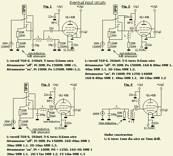
This capacitance must be tuned out if what is adequate drive on 3.5 MHz is to produce full output on the higher-frequency bands. I do this with a dual-circuit (fig1»). By way of flywheel-action this tuned input-circuit will, to a degree, level out the variable input impedance, thereby preserving a reasonable match and thus linearity and output of the driving transceiver. By putting a 50 Ω-swamping resistor across it, the driver will see a load with a SWR of less than 1.5.
With respectively, an input of 100 W, 6 dB attenuation switched "on", 3 kV HT and anode current 0.65 A, the output power with the GU-43B was 1250 W with. With type Q-1P/41 or 42, the power output was 1.3 – 1.4 kW with anode current greater than 0.65 A.
|
|
|
Tube socket with components (see schematic), 3 × 15 nF (red) are removed for the replaced components.
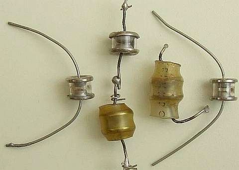
VDR, surge arrestor, varistor, etc.
SCREEN GRID SUPPLY
A screen parallel voltage regulator is a must for a tetrode since the current can flow not only into the grid but periodically out during the driving cycle when the momentary anode potential decreases below the voltage of the screen grid. It is called secondary emission or dynatron effect and it creates a negative internal resistance. The regulator should absorb the current without changing of the supply voltage.
|
Action of the QSK circuit. |
A simplified view of the system, the lamp is used as a constant current device.
High-speed vacuum relay Siemens VR 311, 355 Ω/26.5 V. |
|
NOTE: Connect exclusively the (–Ug2) pole of the not stabilised 470–580 V power supply to point "N". |
|
Transmit and receive switching can be done in couple of ways and it was decided to switch the screen grid voltage (Ug2). The control grid is supplied with a permanent negative voltage of about -52 V and the tube is then "cut off" as there is no Ug2. The negative pole of the screen supply is connected to ground when transistor T2 conduct during transmit via a relay and the 50 Ohm grid swamping resistor. The advantage of this circuit is that a fast-switching relay (for example VR311) with only one contact can be applied. Remember that the negative pole of the stabilised screen supply (point N) must not be connected directly to ground.
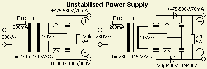
The screen grid is at a stabilised fixed high voltage, if the HV supply fails or the amplifier is not correctly tuned and overloads, the screen grid dissipation is limited to a safe value. To that end, voltage is derived from a non stabilised supply (fig») followed by circuitry comprised of a small 230 VAC/15 W domestic lamp as a constant current device with transistor T1 and serie/parallel connected zener diodes Z as a voltage stabilisation. The transistor has a relatively low amplifying factor (10–15), which eliminates any oscillations. All circuits with many semiconductors or operational amplifiers and a high gain regulation loop (as we may see in publications) are potential source of trouble. In the absence of drive the negative lead N is isolated from ground. E.g. there is almost zero screen voltage and the standing current is very low. During transmit transistor T2 connects the supply's negative pole N to ground. It will be noted that the protected circuitry is incorporated in the main amplifier circuit.
|
|
7 × 6 × 51 V/1.3 W zener diodes. |

This simple circuit works better than expected. If the 27 kΩ resistor is loaded with the 27 kΩ parallel to the screen-grid, the output voltage does not change!
MULTI-PURPOSE FILAMENT TRANSFORMER
|
Control grid, relay and filament supply with single transformer. |
Only one transformer provides the supply for the filament and with rectifying, doubling and quadrupling the supply for the control grid and a fan. Please note that the positive pole is to the ground. A transformer for powering the filament must be exactly suitable for the purpose, not too big and not too small. Use a transformer of 90 W («fig) which provides slightly more than 13 VAC. Measure the voltages of the filament directly on the tube socket and adjust to 12.3 V with a resistor in the primary. That extends the life of the tube.
HV SUPPLY
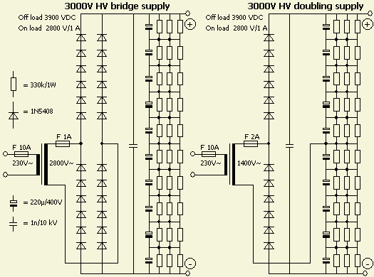
The generation of HV can be done in two ways, with a bridge rectifier and with rectifying and doubling, it depends on the transformer you can get. Many types have a secondary voltage of 1100 - 1300 V or 2200 - 2600 V. Something more is even better with this tube. The unloaded voltage is high but if the amplifier is drive with a continuous carrier (= key down) the voltage drops to a value of the unloaded secondary AC voltage. For example, the DC voltage of a 2800 VAC transformer drops to 2800 VDC with key down. The 220 μF/400 V capacitor shown in the schematics are the most commonly offered for sale on internet.
PI-FILTER
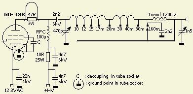
The components of the output pi-filter must be determined empirically for lowest screen current with maximum output power. With normal speech screen current is + 5V to -5V, average Ø Volt, with key down about 20 mA positive. Lowest screen current can be obtained at 3 kV < anode voltage < 3.3 kV.
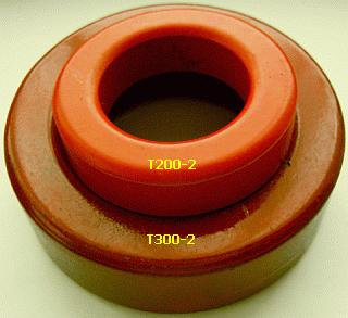
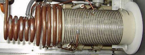
A toroid, self-shielding because of its low external field, facilitates a compact construction of an inductance. Before winding, several layers of Teflon plumbing tape must be applied to the core, to insulate it from the coil-windings. Another method of insulation is to cement two flat isolating washers (e.g. made from bare glass fibreboard, fig») on each side of the bare core. Apply a small quantity of super glue, possibly only a few drops, around the sides of the core. Work swiftly; the glue hardens quickly. The glue prevents the washers from moving out of alignment while the core is being prepared for winding. With a T200-2 core, the inner hole should be 28 mm diameter and the outer diameter 55 mm. With this last construction it might be even possible to use bare copper wire for the windings.
ANODE IMPEDANCE

Normally the anode- or output -impedance is known or can be calculated, or can be taken from a graph. However, hams are in the habit of (miss) using valves in other than normal ways, so available data don't apply. In the past I have built linear amplifiers in a test circuit, following published schematics or design formulae and copying given values of components for a (fig») pi-filter: Ctune, L and Cload. After a while however, one will get an itch to experiment with this or that. Quite often in the following years, output was raised after tinkering with the output circuit. With simple means, the results were measured and tabulated, after which I tried to find a matching formula. I found my results to differ from the formulae and tables as found in handbooks of the years '60. In all probability, pure class B or C was then adhered to. Adjustment according to my "found" formula is a good directive for home-brewing linear amplifiers that are meant for CW and SSB. The anode-impedance of an unknown amplifier's final stage with one or more valves, according to my findings is:
|
Ra = Va ÷ (1.87 × Ia), in which: |
|
Ra = the (common) anode (or plate-)impedance, (in Ohms), |
|
Ia = the (total) anode current at max. power, (in Amperes), |
|
Va = the applied anode voltage, (in Volts). |
One may dispute the value of the last decimal of 1.87, but please consider that it is the average result of many experiments. As it is, the formulae worked very satisfactory for me.
CALCULATION PI FILTER
|
With my formula we find as a suitable anode load (Ra) for : |
Va = 3000 V/0.9 A: Ra = 3000 ÷ (1.87 × 0.9) = 1783 Ω. |
|
The anode-circuit must transfer energy and the circulating current amplification factor Q helps to suppress the generated higher harmonics. A loaded-circuit Q of 10–12 will meet most requirements regarding efficiency, suppression of harmonics and practical values of C and L. If we assume for the 80 m band: |
Q = 10, |
|
then the loaded circuit-impedance becomes: |
Za = Ra ÷ Q = 1783 ÷ 10 = 178.3 Ω. |
|
The tuning-C (=Ct) is mostly responsible for circuit-resonance, which occurs at the frequency for which: |
Zct = 178.3 Ω. |
|
We recalculate to obtain pF's: |
Ct = 106 ÷ 2πfZct, in resp. pF, MHz and Ω. |
|
For 3.5 MHz this becomes: |
Ct = 106 ÷ (2π × 3.5 × 178.3) = 255 pF. |
|
This includes anode capacitance, wiring capacitance and stray capacitance! The circuit transforms the anode-impedance: |
1783 Ω down to 50 Ω, |
|
giving an impedance ratio of: |
1783 ÷ 50 = 35.66 |
|
and a capacitance ratio of: |
√35.66 = 5.97. |
|
The second C, normally called loading-C (=CL), has a value of: |
CL = 255 (pF) × 5.97 = 1522 pF. |
|
Now we calculate the value of L for 3.5 MHz: Across the coil L is the series combination of : |
Ra + Rload = 1783 + 50 = 1833 Ω. |
|
The loaded coil with a Q of 10 will, at resonance, see a resistance of: |
Rs = 1833 ÷ 10 = 183.3 Ω. |
|
Calculating for inductance gives: |
L = Rs ÷ 2πf = 183.3 × (2π × 3.5) = 8.34 µH. |
It can be argued that the calculations with Ra = Va ÷ (1.87 × Ia) formula could be more exact. Just ask yourself what value you should assume for the added capacitance, caused by valve, wiring and stray capacitance's...this uncertainty is much higher than the one caused by a somewhat simpler calculation.
ANODE CHOKE
|
About plate chokes, varying stories circulate. However, least problems arise with one-layer chokes. Because of the dissipation and closeness of the power valves, a heat-resistant coil former is a must: the heat and intense IR-radiation of a power valve at maximum dissipation can make phenol board at 2 cm distance burst out in flames! A sturdy ceramic wire-wound resistor, with its resistance wire removed, will make a good former. A diameter of about 2 cm and a length of 10 cm is satisfactory. Closely wind the former with one layer of 25 – 28 SWG enamelled wires over a length of 5 – 10 cm. In most cases its inductance is sufficient, even at a lowest frequency of 3.5 MHz. To test for series-resonance, short both ends together (fig») and (with a GDO) checks for resonance's in the amateur bands. If there are none, you are lucky. If there are, try to shift them by removing or adding some turns. Another solution is to remove 1 cm of the windings and start again, leaving a gap of 1 cm between windings; then check again. My favourite choke has a diameter of 2 – 2.2 cm, is closely wound over a length of 5 cm with one layer of 28 SWG enamelled wire, has an inductance of about 180 μH and will serve for all bands. The wire may seem too thin for some currents, but in all my experiments it never burnt through. The wirewound resistor (10–50 ?) between +HT and the choke will limit the damage from "flash-over", caused by a momentary short in a valve, to the fuse and (often) the limit-resistor itself. Replacing them is much cheaper than replacing the valve. |
|
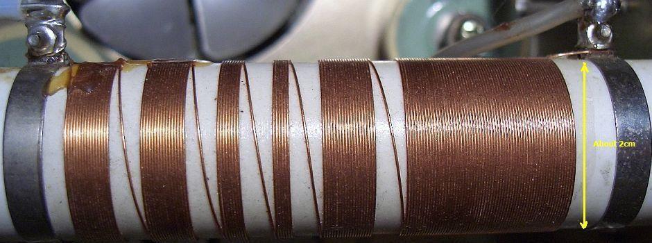
Count turns and make a RFC with the photo as an example.
PROTECTION
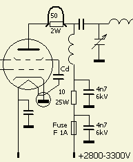
For first protection in all my power amps there is a fuse and a resistor in series with the anode feed (fig»). The wire-wound resistor in the anode-circuit will curtail the flaming arc across the blown fuse and limits the maximum anode current. That proved good practice in this amplifier. Within five minutes after first application of power, there was a flashover in one of the valves. The fuse had blown but the valve had not suffered. Later on, under overdrive, the same thing happened. Again, the valve was OK. Feel free to use a bigger resistor but I use these resistors as a second fuse and do not mind replacing them. It seems that this often occurs with this type of valve after they have not been used for a long time. Once the amplifier has stabilised and is in regular use, this only happens infrequently. An extra 4.7 nF/3 kV bypass capacitor from between the fuse and resistor provides additional filtering.
PARASITIC SUPPRESSION CIRCUITS

A method of parasitic suppression is the insertion of RF current (hairpin shaped) obstacles (dampers) at right angles («fig) to the probable flow of the parasitic currents. This method can be used up to frequencies of several 100 MHz without noticeably reducing fundamental power.
|
Parasitic suppressor. |
The main function is to provide a high impedance path in series with other (tank) circuit elements. However such method can be used only where the fundamental and parasitic frequencies are sufficiently far apart, so that excessive resistive losses of the fundamental frequencies are avoided. The circuit should have a L/C ratio as low as practicable and be suitably damped to give a broadband effect.
Damping can be achieved by paralleling the hairpin circuit inductor with a non-inductive resistor and by making the inductor from resistive material. A mat surface rather than a polished surface may provide sufficient surface resistance. The resistive component need often be no more than a nickel alloy wire/strip or tinned copper wire/strip with a DC resistive value of a fraction of an ohm.
The test amplifier was unconditionally stable without a parasitic suppresser but for safety reasons I placed a stopper as the one shown. I had previously found this type more effective. The 56 Ω/2 W composition resistor (I happened to have that value) is shunted by hairpin loops made of about 2 mm diameter tinned wire. The effective length of the wire is 10 cm but cut off a 12 cm to allow for connection to solder tag. The hairpin size had been optimised on an earlier amplifier and was found to be effective here too.
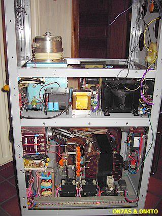
ON7AS & ON4TO
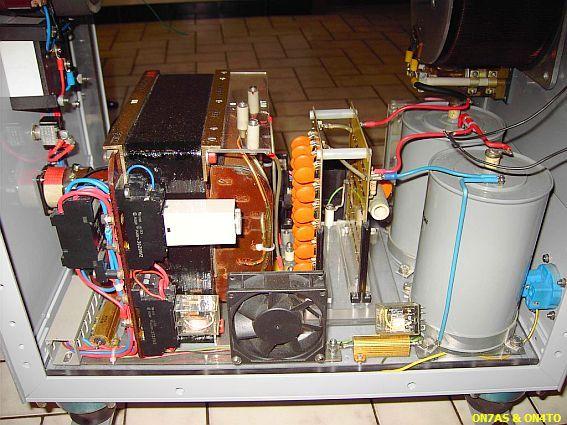
With my design as an example ON7AS and ON4TO made this huge amplifier two times.
|
|
|
SOCKET
Shown are examples of sockets for a GU-43B.
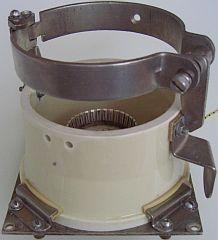
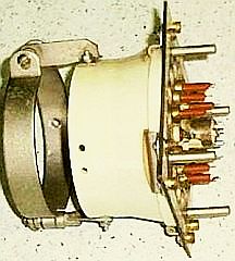
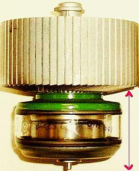
1st type socket
NOTE: With some brands GU-43B the dimension from anode to base is about 5 mm that is to short for this chimney/socket, it is impossible to supply 12 V to the filament connector of the valve.

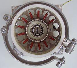
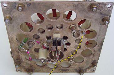
2nd types socket (see 12 × red 15 nF feed-through capacitors).
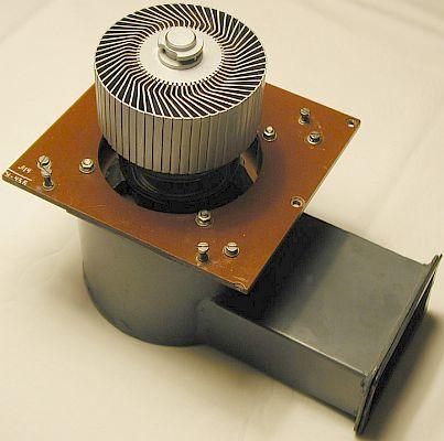
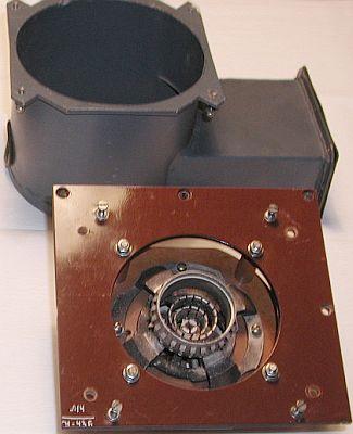
3rd type socket and chimney.
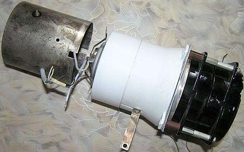
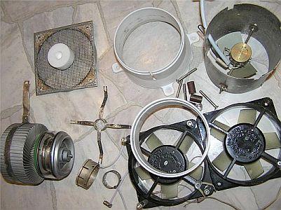
4th type socket and chimney.
4L1DA's & UY5ZZ's GU-43B AMPLIFIER
|
4L1DA's design, see the differences with UY5ZZ's and PA0FRI's PA's below.
UY5ZZ's commercial design, see the differences with PA0FRI's PA design below.
PAØFRI's 1st design |
SOME HOME MADE COMPONENTS FOR THE FRINEAR 1500
|
|
|
At present my second chimney is home made with standard PVC tubes, cooling with 12 × 12 cm fan.
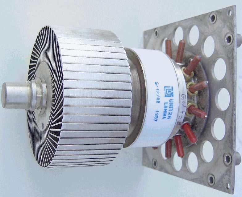
Room for all components?